


Cleanrooms for Semiconductor Production
In the fast-paced landscape of advanced manufacturing and technological innovation, one element stands as the cornerstone of precision and excellence: Semiconductor Cleanrooms. These controlled environments play a pivotal role in shaping the modern world by ensuring the flawless production of microchips and semiconductor devices that power our interconnected lives. Instant Cleanroom Solutions has recently dispatched its seventh cutting-edge Instant Cleanroom™, accompanied by one Mobile Cleanroom, in a resounding show of support for contractors engaged in the groundbreaking TSMC (Taiwan Semiconductor Manufacturing Company) semiconductor fabrication project in Arizona. Keep reading to learn more on the intricacies of these pristine environments, shedding light on their purpose, design principles, and the pivotal role they play in driving the semiconductor industry forward.
Understanding Semiconductor Cleanrooms
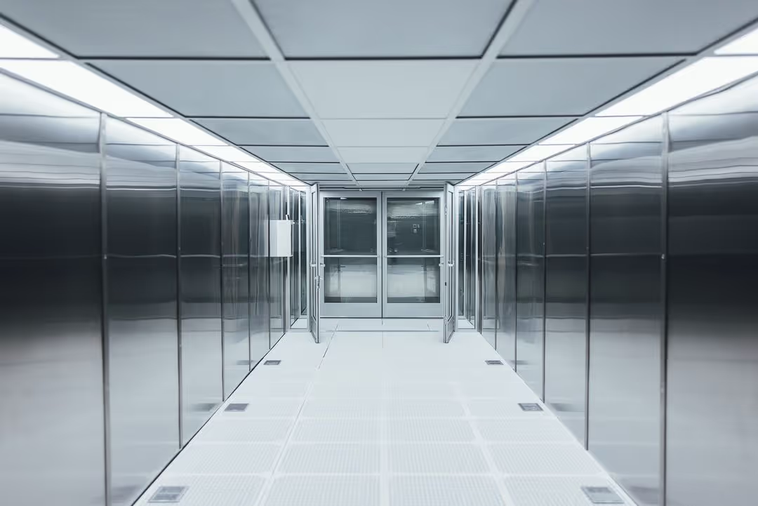
At its core, a semiconductor cleanroom is a highly specialized and controlled environment engineered to maintain an exceptionally low level of airborne contaminants. These contaminants, which could include particles as small as a fraction of a micron, have the potential to adversely impact the delicate processes involved in semiconductor fabrication.
Cleanrooms Importance in Semiconductor Manufacturing
The significance of semiconductor cleanrooms in the realm of manufacturing cannot be overstated. Every step in the production of microelectronic components demands an environment free from impurities that could compromise the final product's quality and functionality. From photolithography and etching to thin-film deposition and wafer inspection, every intricate procedure requires the precision and purity that only a cleanroom can provide. The absence of contaminants ensures that the resulting microchips meet the highest standards of performance and reliability, thus driving the innovation and growth of the semiconductor industry.
Impact on Overall Yield and Performance
The impact of semiconductor cleanrooms extends beyond individual microchips – it resonates through the entire landscape of semiconductor manufacturing. Cleanrooms play a pivotal role in elevating the overall yield and performance of manufacturing processes. As impurities are systematically eliminated, the production line is liberated from potential setbacks caused by defects and inconsistencies. This, in turn, boosts yield rates, leading to a higher quantity of fully operational microchips. The ripple effect is felt across industries that rely on these microchips, from consumer electronics to medical devices, empowering technological progress on a global scale.
Key Features and Design Principles
Particle Filtration and Airflow Control
The heartbeat of a semiconductor cleanroom lies in its advanced particle filtration and airflow control systems. high-efficiency particulate air (HEPA) filters take center stage, strategically placed throughout the cleanroom to capture and eliminate even the tiniest particles that traverse the air. These filters operate in tandem with sophisticated airflow control mechanisms, ensuring a consistent and uniform distribution of pristine air. The result is an environment where the air itself is purified to an extraordinary degree.
Temperature and Humidity Regulation
Temperature and humidity regulation within cleanrooms play an important role in maintaining the delicate balance necessary for flawless manufacturing processes. Advanced heating, ventilation, and air conditioning (HVAC) systems work tirelessly to achieve and maintain the exact temperature and humidity levels required for optimal production. The controlled environment ensures that variations are minimized, guarding against deviations that could compromise the precision of microchip fabrication.
Cleanroom Garments and Protocols
While technology forms the backbone of semiconductor cleanrooms, the human element remains equally crucial. Cleanroom personnel adhere to stringent gowning procedures, donning specialized garments such as cleanroom suits, gloves, and masks. These attire essentials form a barrier against human contamination, safeguarding the integrity of the manufacturing environment. Moreover, meticulous protocols for entering and exiting the cleanroom are strictly enforced, leaving no room for compromise when it comes to maintaining the desired cleanliness levels.
Cleanroom Layout and Zoning
The layout of a semiconductor cleanroom is a carefully orchestrated design focusing on efficiency and contamination control. Different areas within the cleanroom are meticulously zoned based on varying cleanliness requirements. Each zone is tailored to the specific tasks carried out within, ensuring that the degree of cleanliness aligns with the demands of the processes at hand. This strategic zoning minimizes the risk of cross-contamination and optimizes workflow, enhancing overall efficiency and contributing to the production of microchips.
Exploring the Semiconductor Cleanroom Workflow
A. Reception and Gowning Area
The journey begins at the reception, a gateway to the world of semiconductor cleanrooms. Here, personnel transition into the realm of controlled environments, donning the specialized garments that render them impervious to contamination.
B. Material Entry and Preparation Zone
As individuals step further into the cleanroom, the material entry and preparation zone unfolds. This is where the raw materials, the lifeblood of semiconductor production, make their entrance. The materials undergo meticulous scrutiny and preliminary processes to ensure they meet the stringent cleanliness standards demanded by the manufacturing processes that lie ahead.
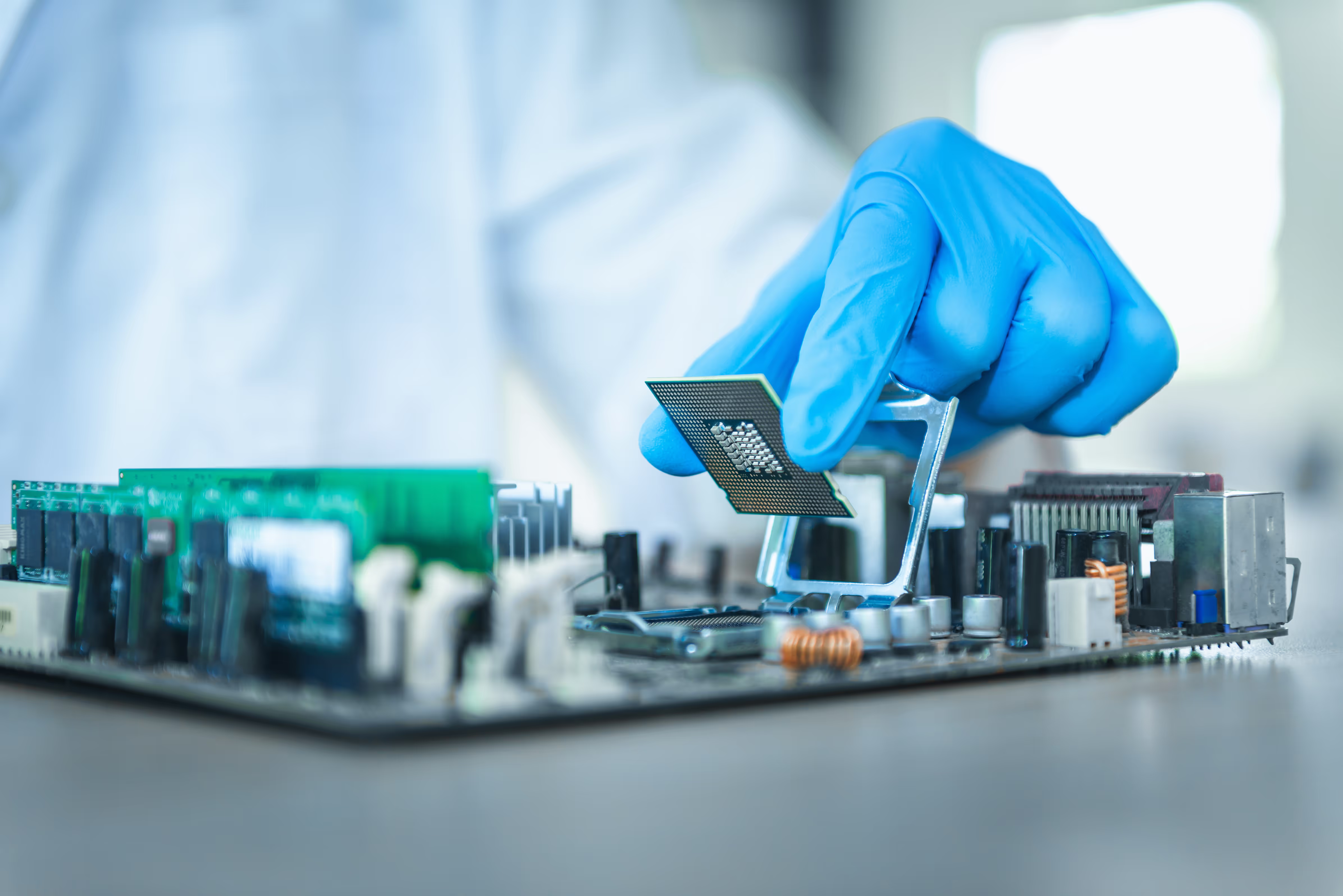
C. Wafer Fabrication and Assembly & Testing
The heart of the cleanroom lives in the wafer fabrication and assembly & testing zones. Here, precision equipment dances in harmony, etching intricate patterns onto wafers with unparalleled accuracy. Each microchip is subjected to rigorous assessments to ensure its flawless functionality.
D. Packaging and Material Exit
From assembly to packaging, the cleanroom continues to protect the microchips. In the packaging zone, the precious components are encapsulated with care, safeguarding their integrity as they prepare to go beyond the controlled confines.
E. Quality Control and Storage
Here, the microchips undergo a final series of meticulous tests to ensure they meet the exacting standards that define semiconductor excellence. Once approved, they are ushered into the storage area, awaiting deployment to power the technologies that drive our interconnected world.
Conclusion
In the dynamic landscape of semiconductor production, cleanrooms emerge as the indispensable bedrock of precision and advancement. These meticulously controlled environments exemplify the paramount importance of maintaining immaculate conditions for manufacturing processes. Each step within a cleanroom's design and use contributes to the creation of microchips and integrated circuits that pave the way for advancements that shape our future.
If you want to learn more about our Instant Cleanroom™ or Mobile Cleanrooms that are being used for the construction of semiconductors fabs please click the links, or email one of our experts today.